Markets Flexibel e-beam solutions for a huge variety of applications

Markets Flexibel e-beam solutions for a huge variety of applications

Markets

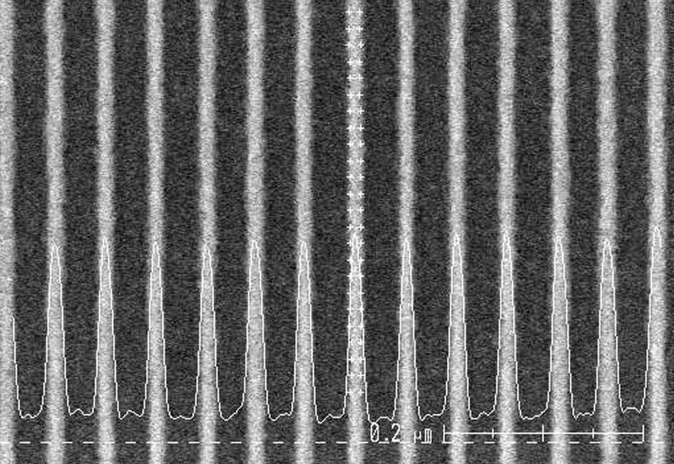
Electron Beam Lithography is a key enabling technology for both Semiconductor and Micro/Nano fabrication. With Variable Shaped Beam technology and a high degree of automation, our systems are tailored for use in applied research and industrial production, where reproducible and fast exposures of entire substrates or stacks with high quality are required. 

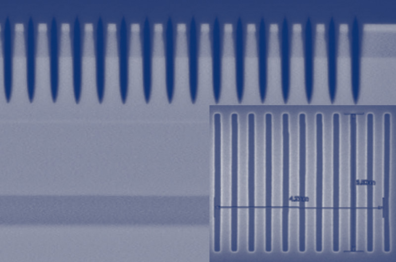
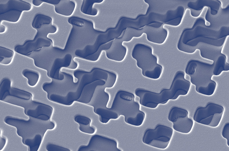
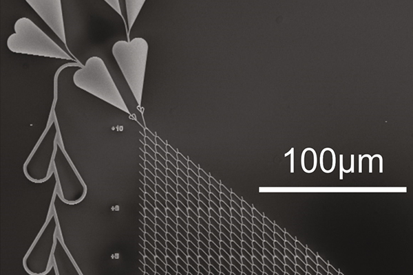
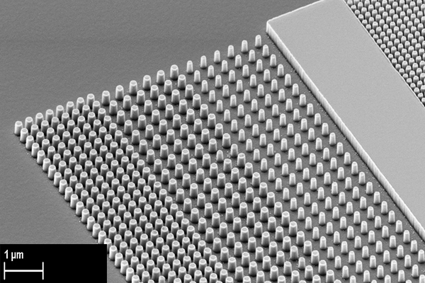
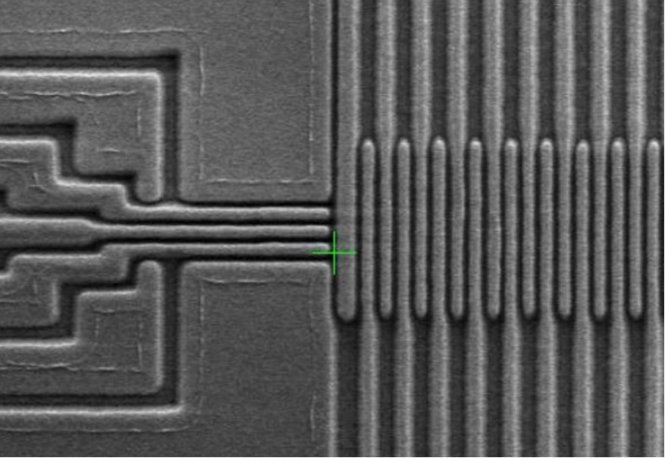
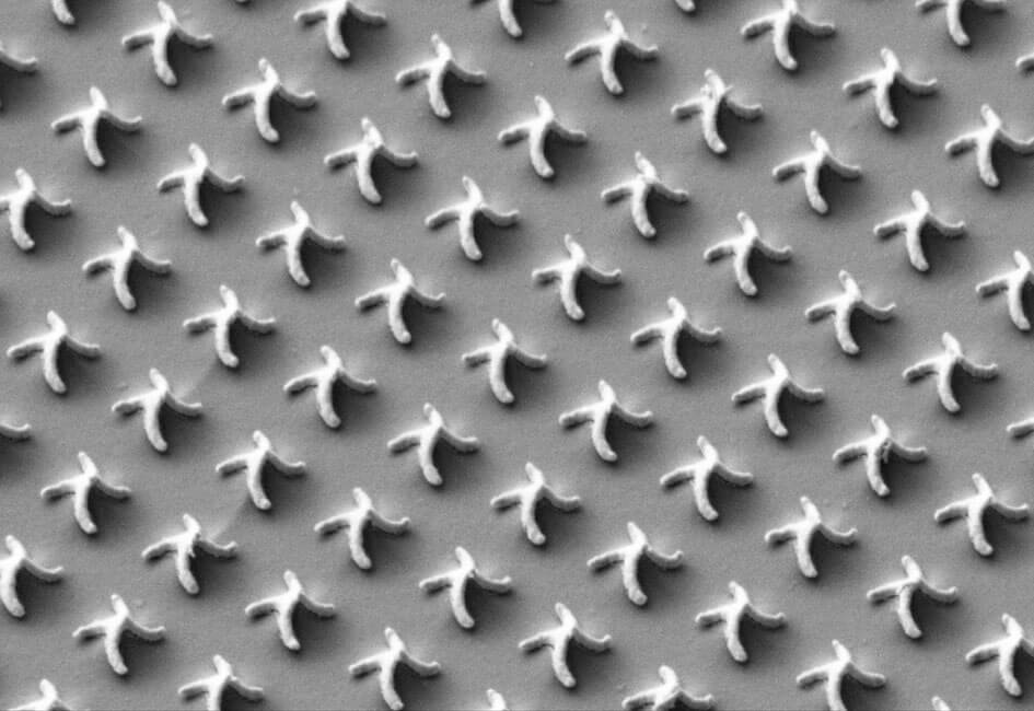
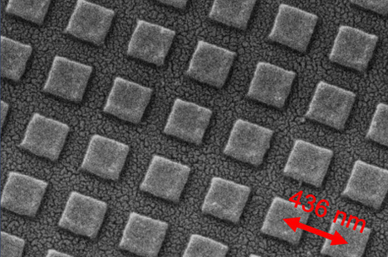
Applications range from micro- and nanoelectronics to integrated optics and photonics to nano- and biotechnology. Arbitrary layouts can be written directly on wafers or masks with high resolution, e.g. microelectronics circuits, diffractive optical elements, or metamaterials. 

Efficient data processing & extended strategies open up new applications, especially in the field of AR/VR. 

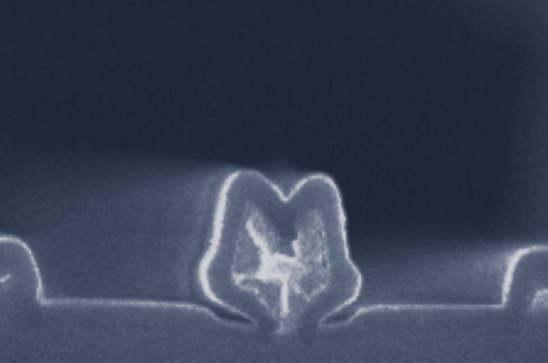
Maskless writing with the electron beam enables high flexibility to generate new devices, small volume production, writing of critical features in multilayer devices, or generation of templates for mass production.

Our lithography systems are mainly used in three markets

Applications

  • Aerospace & defense
  • AR & VR applications
  • Biosensing, spectroscopy
  • CMOS applications
  • Diffractive optical elements
  • Early device evaluation
  • Emerging applications
  • Fast prototyping
  • Foundry services
  • Functionalized surfaces
  • Holograms
  • Industrial Compound Semiconductor production
  • Industrial production of masks for optical lithography
  • Integrated optics and photonics
  • Laser gratings
  • Logic & memory
  • MEMS / NEMS
  • Metamaterials
  • Micro-optics on glass
  • Micro-optics
  • Mid-range technology nodes
  • Mix & match with optical lithography
  • Network infrastructure
  • Optical proximity correction
  • Optoelectronics
  • Projection lighting
  • Prototyping
  • Quantum computing
  • Quantum technologies
  • RF transistor electronics
  • Silicon direct write
  • Silicon Photonics
  • Telecom & data centers
  • Template manufacturing
  • Various applications in nanopatterning

Compound Semiconductor

Our lithography systems are capable to directly pattern a huge variety of compound semiconductor materials with high reliability & stability which are needed in 24/7 production environments. Moreover, we offer the flexibility to use different substrate types at our machines and fully automated handling and alignment procedures for overlay exposures.
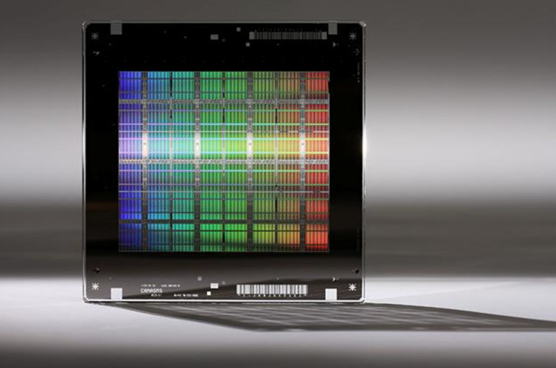
Mask and Glass

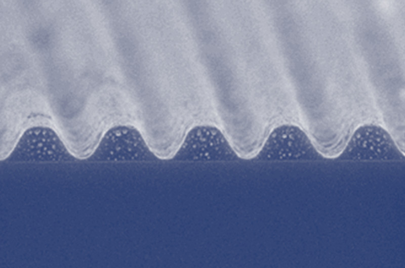
We provide e-beam lithography systems for industrial mask makers. Moreover, micro-optical elements can be patterned onto glass substrates with excellent quality and high accuracy. Another application is template writing to enable mass production of small structures, e.g. for metasurfaces, on large areas.

Advanced Research

Our customers in research institutions typically operate multi-user facilities. They use our electron beam lithography systems to manufacture devices for multiple emerging applications like quantum computing, MEMS/NEMS technology or biosensing. The high flexibility of the Vistec systems and the capability for efficient writing on large areas are of particular importance for our customers.

Applications

  • III-V Device

    T-Gate (Device Sample) 
    System: Vistec SB250 
    Source: WIN Semiconductors Corp., Taiwan

  • Gratings

    AlGaAs waveguide (DFB Laser) 
    System: Vistec SB250 series 
    Source: Ferdinand Braun Institute, Germany

  • Mask Patterning

    Mask Patterning up to 9 inch
    System: Vistec SB3XX Series
    Source: Photronics MZD GmbH, Germany

  • Mask Patterning

    Multilevel Photomask
    System: Vistec SB350 OS
    Source: Fraunhofer IOF, Germany

  • Biophotonics

    Network-based biocomputation (detail)
    System: Vistec SB254
    Source: Fraunhofer ENAS, Germany

  • 3D Patterning

    3D resist profile
    System: Shaped Beam Series
    Source: Vistec, Germany

  • Semiconductor

    Pillars Ø 500 nm, h: 1.5 μm on 15 μm pedestal
    System: Vistec SB352 HR
    Source: IMS Chips, Germany

  • Optics

    Nano-Imprint Master for optical Metasurface
    System: Vistec SB350 OS
    Source: Fraunhofer IOF, Germany

  • Qubits

    Silicon-based Qubits; 80nm pitch
    System: Vistec SB3050 DW
    Source: Fraunhofer IPMS CNT, Germany

  • Cell Projection

    Cell Projection using 1.5 μm x 0.75 μm cell size
    System: Vistec SB3054
    Source: STMicroelectronics, CEA-LETI, France

  • Resolution Capability

    10 nm lines
    System: Vistec SB3xx
    Source: Vistec

  • Chiral optical structures

    Cell Projection
    System: Vistec SB350 OS
    Source: Fraunhofer IOF

  • Plasmonic metasurfaces

    Cell Projection
    System: Vistec SB350 OS
    Source: IPHT Jena

Contact

Contact Form


Privacy Statement