We are really stoked that two of our collegues won the "Best Photon Micrograph" at the EIPBN 2026 Micrograph Contest sponsored by Zyvex Labs. Check it out here: eipbn.org/micrograph-contest/
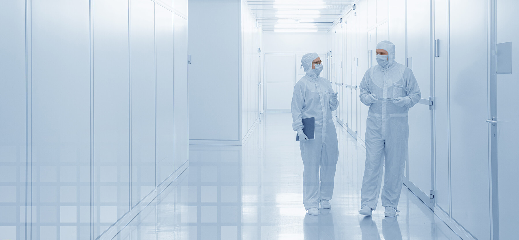
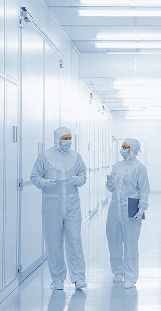
Today we hosted a group of students from the Carl Zeiss Gymnasium Jena. Our boss gave them a personal tour of the clean room and explained what variable shaped beam electron beam lithography is and what our lithography equipment is used…
In the T1 Poster-Session on Wednesday "Micro/nanostructuring" Sep 18th, starting 4.30pm we'll present "Tuning the optical performance of photonic structures by optimized Variable Shaped Beam lithography"
At the Semicon West exhibition our team will be available to present and discuss our recent Variable Shaped Beam lithography products and technologies, data preparation and Cell Projection.
Investment in new production tool for the semiconductor equipment industry.
Jenoptik is investing a low double-digit million-euro amount in a state-of-the-art system for the high-tech fab currently under construction in Dresden. The new…