

A brief look at
Vistec Electron Beam’s history

60 years ago a group of engineers at Carl Zeiss in Jena began exploring the possibilities of using electrons for microlithography, based on their experiences with electron microscopy.
30 years ago, in March of 1996, the “Microlit Division of Jenoptik Microfab GmbH” (the former Zeiss E-Beam Lithography division) was sold to Leica Microsystems and became Leica Lithographie Systeme Jena GmbH. After further transitions this 1996 born E-Beam-company bears the name Vistec since 2005 and jonied the HEIDENHAIN Corporate Group in 2012.
Throughout this long history hundreds of Variable Shaped E-Beam Writers were shipped worldwide. The core technology has remained in these systems but the technology has continued to be improved and refined.
Today Vistec's E-Beam-Writers feature seamless integration of Variable Shaped Beam and Cell Projection lithography. The systems have proven to be the most flexible and manufacturing robust tools available in today’s world market.
Vistec’s Electron Beam lithography tools are employed in many applications such as applied research, fab production direct wafer writing, photomask writing and photonics / microoptics.
Vistec's engineers are proud to deliver custom tailored nano-writers in application specific configurations for various fully automatically handled substrate materials and types such as 100 to 300 mm wafers, up to 9” masks and even small coupons, all on the same tool without engineering changeovers.
Do not hesitate to ask us for more information - We Understand E-Beam.
Get to know us
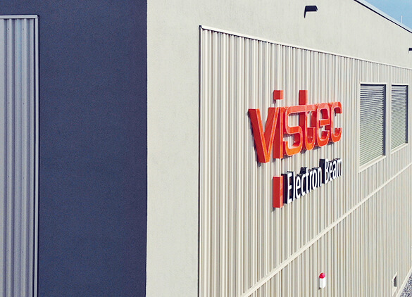
Our Company
Vistec Electron Beam is a leader in the design and manufacturing of electron-beam lithography systems, which are based on the Variable Shaped Beam (VSB) principle. In conjunction with extended writing strategies and efficient layout data processing the electron-beam lithography systems are capable to fully expose 300 mm wafers and 9 inch masks on the same platform. The application areas span a wide range of existing and emerging applications including silicon direct write, compound semiconductor, mask making, advanced research, integrated optics and photonics for customers in both industry as well as Advanced Research.
Our History
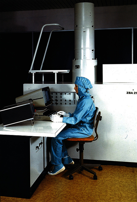
The company's roots go back to Carl Zeiss Jena in the early 1970s, when the first commercial electron-beam exposure system based on the VSB principle was introduced. The main customers for the so-called ZBAs (Zeiss exposure system) were the former RGW (Rat für gegenseitige Wirtschaftshilfe - Council for Mutual Economic Assistance) countries. After the political changes in Germany, electron beam lithography was initially continued under the roofs of JENOPTIK and later Leica Microsystems. Since 1996, Leica Electron Beam Lithography has been operating as a limited liability company (GmbH). As a result of a restructuring process in 2006 the company had to change the name in Vistec Electron Beam. Since 2012, Vistec Electron Beam GmbH has been a member of the HEIDENHAIN Corporation Group.
The company employs more than 110 people worldwide. The headquarter is located in Jena, Germany, with offices and manufacturing facilities for assembly and qualification. In addition to their production facility in Germany, Vistec maintains service and support centres in Europe, China, Taiwan and also in the US.
Thanks to its location, Vistec Electron Beam benefits from the synergies between leading edge research institutes, small and mid-sized equipment and supplier companies as well as key semiconductor manufacturers in the neighborhood area.
Vistec is certified by DIN EN ISO 9001:2015.
Company Milestones
-
2021
-
2012
-
2005
-
1996
-
1990
-
1974